Product Introduction
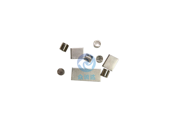
Indium is a soft, silver-white metal with excellent ductility and malleability. It is widely used in thin film evaporation and sputtering processes. Indium deposition materials are typically provided in high-purity metal block or particle form and can form uniform and dense films through vacuum evaporation, electron beam evaporation, or magnetron sputtering processes. Indium thin films have excellent electrical conductivity and adjustable optical properties, making them key materials for transparent conductive films, semiconductor devices, and high-end optoelectronic devices.
Outstanding Characteristics of Indium
High Purity
Indium deposition materials can reach a purity of 99.99%, with very low impurity content, ensuring stable and reliable film performance.
Good Electrical Conductivity
Indium thin films have low resistivity and can be used for transparent conductive films and electrode materials.
Excellent Ductility and Workability
Indium is soft and easy to process, allowing for the formation of uniform, dense films with good adhesion.
Excellent Chemical Stability
Indium has excellent corrosion resistance in most environments, ensuring long-term stability of devices.
Wide Applications of Indium
Displays
Indium is used to produce indium tin oxide (ITO) films, widely applied in LCDs, touchscreens, and OLED displays.
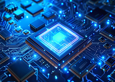
Semiconductor Manufacturing
Indium is used as contact electrodes or functional thin films, improving device performance and stability.
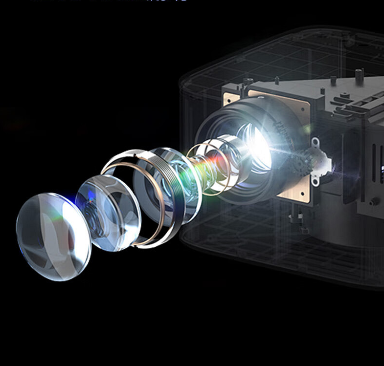
Optoelectronic Devices
Indium is used in photovoltaic cells, photodetectors, and laser devices, enhancing photoelectric conversion efficiency.
Used as high-k dielectric films in the semiconductor field, meeting the miniaturization and high-performance requirements of chips.
Technical Characteristics

Purity:
99.99% - 99.999%
Application Fields
Optical Device Manufacturing

Photovoltaic Industry
Semiconductor Manufacturing
Contact Us