Solution
Semiconductor
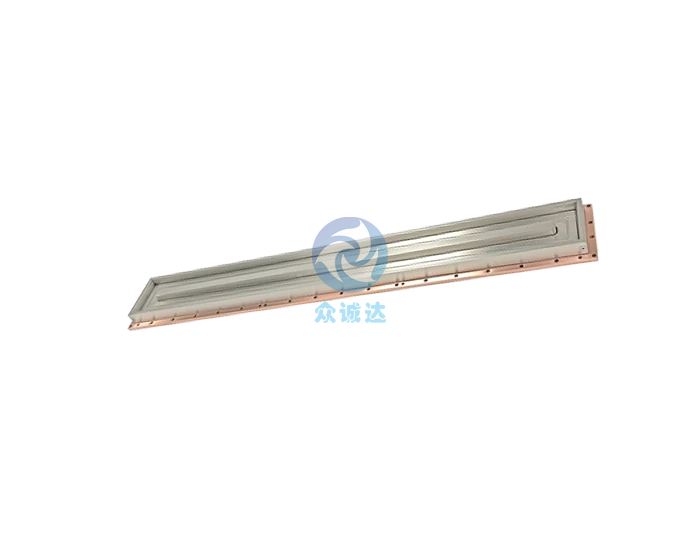
Main Target Materials:Cu,Ti, W, SS, AI, Si, Ni, Mo, Cr, Ta, Ag, Au, Pt, Ir, Sc, AISC, NiFe, NiCr, NiCu, WTi, AICu, PZT, LNO, NiV
Evaporation Materials:Cu, Ni, Ti, W, AI, Mo, Cr, Ta, Ag, Au, Pt, Ir, Y
These target materials are critical and indispensable components in semiconductor manufacturing. They are widely utilized across advanced packaging, third-generation semiconductors, MEMS devices, and various electronic components. Through physical vapor deposition (PVD) sputtering, these materials form essential conductive, barrier, insulating, and functional films on wafer and substrate surfaces. This process significantly enhances device performance, reliability, and manufacturing yield, while consistently meeting the stringent requirements for film thickness uniformity and stability demanded by advanced semiconductor processes.
1.Advanced Packaging
In advanced packaging processes, including flip-chip, fan-out packaging, and 3D stacking, target materials are used to deposit critical layers such as metal interconnects, diffusion barriers, and re-routing layers (RDLs). These materials are instrumental in boosting packaging density, increasing signal transmission speeds, and improving thermal management capabilities, all while ensuring superior film adhesion and long-term device reliability.
2.Third-Generation Semiconductors
In the manufacture of third-generation semiconductor power devices like Silicon Carbide (SiC) and Gallium Nitride (GaN), target materials are used to create electrodes, barrier layers, protective films, and various functional films. These materials maintain excellent conductivity and structural stability in high-temperature, high-pressure, and high-frequency environments, thus meeting the stringent durability and stability requirements of modern power devices.
3.MEMS Devices
Target materials are used to deposit sensitive films, functional films, and protective films in the manufacture of MEMS (Micro-Electro-Mechanical Systems) devices such as pressure sensors, accelerometers, and gyroscopes, , ensuring high sensitivity, reliability, and stability at the microscale.
4.Electronic Components
In the production of various electronic components—including capacitors, resistors, sensors, and switches—target materials are utilized to form critical conductive layers, dielectric layers, and packaging protection layers. These materials effectively enhance electrical conductivity, improve insulation properties, and increase environmental durability, thereby extending component lifespan and ensuring stable, reliable performance.
Key Roles
Ensure Stable Film Performance
Enhance Device Reliability
Support The Development Of Advanced Processes
Promote Green Manufacturing And Cost Optimization